The birth of 3D Flash Memory “BiCS FLASH™”
Kioxia's predecessor, Toshiba, successfully developed NAND flash memory in 1987 and became the first in the world to mass-produce it in 1991. Through design guidelines and processes, the capacity of NAND flash memory has been continuously improved.
However, increasing the capacity of NAND flash memory within the limitations of planar processes has become very challenging.
To address the issue of insufficient memory storage, Kioxia employed new technology to vertically stack flash memory chips and announced 3D flash memory stacking technology in 2007. Building on this foundation, Kioxia further developed related technologies and introduced 3D flash memory: BiCS FLASH™.

Key Features
High storage density and high capacity
2D NAND refers to adding BiCS FLASH™ cells on a limited planar surface. However, as demand and technology evolve, the number of cells that can be arranged in a planar mode is quite limited. This technological advancement trend has led to the birth of 3D NAND technology.The new 3D NAND technology is based on 2D NAND but shifts from a planar to a three-dimensional structure. This significantly increases the space available for stacking BiCS FLASH™ cells, thereby greatly expanding storage capacity.
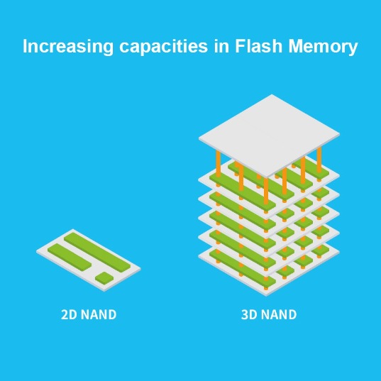
By employing a 3D stacked structure, the distance between BiCS FLASH™ cells is significantly increased compared to 2D NAND. This reduces the variability of memory cells, speeds up data interpretation for each write sequence, and results in faster write speeds.
High stability
Compared to the difficulty and reliability issues of planar shrinking in 2D NAND, the vertical stacking technique in 3D NAND significantly increases the distance between BiCS FLASH™ cells. This increased distance reduces interference between cells, thereby enhancing stability.
Low Power Consumption
BiCS FLASH™ enhances the data volume of write sequences and noticeably improves processing speed. Compared to 2D NAND, it significantly reduces the energy consumption required for data processing, making it more energy-efficient.
BiCS FLASH™ Technologies
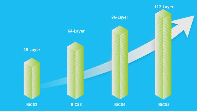
From the initial BiCS1, through improvements and new processes, BiCS3 was finally installed in computers. Today, BiCS5 is widely used, and with the technology now relatively mature, the unit cost of each NAND has decreased while the storage capacity per unit has increased, achieving optimal cost-efficiency.
5th-Generation BiCS FLASH™
In 2020, KIOXIA and Western Digital introduced the BiCS5 112-Layer 3D NAND, which outperforms the BiCS4 96-Layer 3D NAND. Compared to its predecessor, the advanced stacking technology of BiCS5 increases storage capacity per unit by nearly 40%. Alongside increased storage capacity, performance has significantly improved, unit costs have decreased, and energy consumption is lower. Experimental data shows that BiCS5's I/O performance is nearly 50% better than BiCS4.
NAND FLASH Applications
For the industry as a whole, flash memory drives the evolution of Industry 4.0. Artificial intelligence and 5G IoT rely on flash memory for data management, storage, and transfer, facilitating industry transformation and development. These technologies are being applied to realize the vision of autonomous driving and personalized medical services within healthcare systems, gradually developing into smart cities.


__24C15hqqtC.png)
__24C15wOdCC.png)



__24C05XQ2my.jpg)




__24C05fplcZ.png)
__24C05vgHYC.png)
